The term “nanotechnology” was first used by Norio Taniguchi of the Tokyo Science University in 1974. Taniguchi used the word to refer to “production technology to get the extra high accuracy and ultrafine dimensions, i.e. the preciseness and fineness on the order of 1 nanometer.”
(“On the Basic Concept of Nanotechnology,” Proceedings of the International Conference of Production Engineering, 1974)
1974: Molecular Electronics
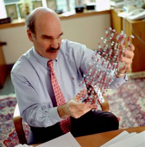
Mark A. Ratner, Northwestern University Charles and Emma Morrison Professor of Chemistry, and A. Aviram of IBM proposed that individual molecules might exhibit the behavior of basic electronic devices, thus allowing computers to be built from the bottom up by turning individual molecules into circuit components.
This hypothetical application of nanotechnology, formulated long before the means existed to test it, was so radical that it wasn’t pursued or even widely understood for another 15 years.
For this groundbreaking work, Ratner is widely credited as the “father of molecular-scale electronics,” and his contributions were recognized in 2001 with the Feynman Prize in Nanotechnology.
(Chem. Phys. Lett. 29, 277, 1974)
1977: Surface Enhanced Raman Spectroscopy (SERS)
Some of the tools needed in the field of nanotechnology were many years in the making. For example, spectroscopy is a set of techniques that use the interaction of light with matter to obtain information about its identity and structure of molecules.
Sir Chandrasekhara Venkata Raman (Calcutta University) won the 1930 Nobel Prize in Physics for his 1928 discovery that the scattering of light by molecules could be used to provide information about a sample’s chemical composition and molecular structure.
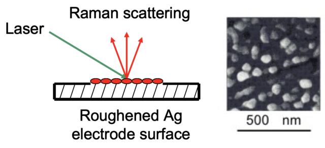
Although a ground-breaking technique, Raman Spectroscopy was not capable of detecting at the nanoscale. The technique was greatly improved in the 1960s by the invention of the laser, but it wasn’t until 1977, when Richard P. Van Duyne (Northwestern University) discovered Surface Enhanced Raman Spectroscopy, that nanoscale studies became possible.
Van Duyne deduced that when molecules were attached to a surface which had hills and valleys that were approximately 50-100 nanometers in size, the Raman intensity was amplified 1,000,000 times.
The discovery of SERS completely transformed Raman Spectroscopy from one of the least sensitive to one of the most sensitive techniques in all of molecular spectroscopy. Today, SERS is used to study the chemical reactions of molecules in electrochemistry, catalysis, materials synthesis, and biochemistry. The sensitivity of SERS is now so high that even single molecules can be studied.
1980: Self-Assembled Monolayers (SAMS)
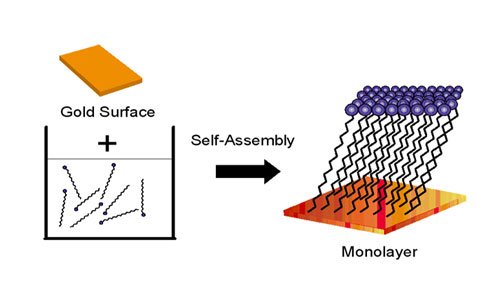
In 1980, Jacob Sagiv at the Weitzman Institute in Israel discovered that molecules containing a chemical called octadecyl trichlorosilane, or OTS, would spontaneously react with a glass surface to assemble by themselves into individual layers.
In 1983, a Bell Labs research team lead by David Allara discovered that molecules with thiol groups (groups containing sulfur) on a gold surface would also self-assemble into individual or mono-layers. These self-assembled monolayers are typically a few nanometers thick (determined by the choice of molecule) and allow researchers to tailor the properties of a surface.
For the first time, scientists could envision building three-dimensional nanoscale structures layer-by-layer, like laying rows of bricks to build a wall. These structures are being used to build molecule-based electronic devices, biosensors, and new types of optical materials.
(Sagiv, J. J. Am. Chem. Soc., 102, 92-98, 1980)
(J. Am. Chem. Soc., 105, 4481, 1983)
1981: Scanning Tunneling Microscope
In 1981, the scanning tunneling microscope was invented by Gerd Binning and Heinrich Rohrer at IBM’s Research Laboratory in Zurich Switzerland. This invention allowed scientists to not only observe nanoscale particles, atoms, and small molecules, but to control them.
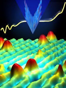
The STM scans the tip of a needle, or “probe,” just a few atoms above the surface of the sample. A voltage is applied between the tip of the probe and the surface. As the electric current begins to flow, the STM can determine minute variations in the distance electrons travel. In this way, the STM maps the surface of the sample. The information is saved in a data file, and a “picture” of the surface is created by the computer.
In this way, the STM can “see” atomic-scale objects. The STM helps researchers determine the size and form of molecules, observe defects and abnormalities, and discover how chemicals interact with the sample.
The STM quickly became standard equipment in laboratories throughout the world. Binning and Rohrer were awarded the Nobel Prize in physics in 1986 along with German scientist Ernst Ruska, who designed the first electron microscope.
(US Patent #4,343,993)
The “Buckyball”
Another nanotechnology breakthrough occurred in 1985, when Richard Smalley, Robert Curl, and graduate student James Heath at Rice University and Sir Harry Kroto at the University of Sussex discovered C60, a carbon nanoparticle shaped like a soccer ball.
The unique molecule was named Buckminsterfullerene after the visionary American architect and engineer Buckminster Fuller, who designed the geodesic dome. More commonly called a “buckyball,” the molecule is extremely rugged, capable of surviving collisions with metals and other materials at speeds higher than 20,000 miles per hour.
Because of this ruggedness, buckyballs show promise in the development of fuel cells that might power the automobiles of the future. Researchers are also investigating the possibility of using buckyballs as tiny drug delivery systems. Smalley, Curl, and Kroto won the 1996 Nobel Prize in Chemistry “for their discovery of fullerene.”
(J. Phys. Chem., 90, 525-528, 1986)

1986: Atomic Force Microscope
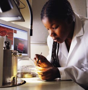
Invented by Gerd Binnig and his colleague Christoph Gerber at IBM and Calvin Quate at Stanford University, the atomic force microscope (AFM) uses a cantilever to “read” a surface directly, the way a record player’s needle reads a record.
Atomic force microscopy works by passing the cantilever – so sharp that its tip is composed of a single atom – within a few nanometers of a surface. The atomic forces exerting a pull on the cantilever are measured to create an atom-by-atom topographical map.
The AFM makes 3D images of an object’s surface topography with extremely high magnifications (up to 1,000,000 times).
(Phys. Rev. Lett., 56, no. 9; 3; p.930 3, 1986)
1987: Single Electron Tunneling Transistor
In 1987, Dmitri Averin and Konstantin Likharev, then at the University of Moscow, proposed the idea of a new device called a single-electron tunneling (SET) transistor.
Two years later, Theodore Fulton and Gerald Dolan at Bell Labs in the US built such a device. In this structure, the controlled movement of individual electrons through a nanoscale device was first achieved.
Single-electron devices are based on what is called the tunnel effect. When two metallic electrodes are separated by an insulating barrier about one nanometer thick (approximately 3 atoms in a row), the electrons are able to “tunnel” through the insulator, even though classical theory suggests that this is impossible.
Researchers have long considered whether SET transistors could be used for digital electronics, but the random variations in voltage from device to device caused serious problems.
Working at the nanoscale, today’s researchers are considering how to overcome this problem by combining all of the components of the SET transistor into a single molecule. It is possible that conventional circuits will one day be replaced by electronics based on individual molecules and form the basis for a new class of nanoelectronics.
(Theory – DV Averin and KK Likharev, J. Low Temp. Physics. 62, 345, 1986)
(Demonstrated – TFulton and GJ Dolan, Phys. Rev. lett. 59, 109, 1987)

Discovery of Quantum Dots
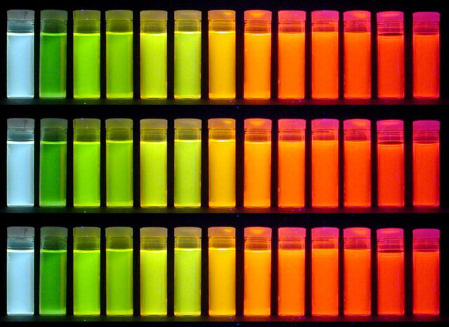
In the early 1980s, Dr. Louis Brus and his team of researchers at Bell Laboratories made a significant contribution to the field of nanotechnology when they discovered that nano-sized crystal semiconductor materials made from the same substance exhibited strikingly different colors.
These nanocrystal semiconductors were called quantum dots, and this work eventually contributed to the understanding of the Quantum Confinement Effect, which explains the relationship between size and color for these nanocrystals.
Due to their extraordinarily small size, the electrons inside the quantum dots exhibit unique behavior. Specifically, the electrons are confined to far fewer energy levels than allowed in bulk semiconductor materials. As a result, the quantum dots emit very intense light of a specific color when the electrons make transitions between these discrete energy levels. Small differences in the size of the quantum dot change the allowed electron energies and therefore alter the color of light which they emit. Scientists have learned how to control the size of the quantum dots, making it possible to obtain a broad range of color (see Medieval Period and stained glass).
Quantum dots have the potential to revolutionize the way solar energy is collected, improve medical diagnostics by providing efficient biological markers, and advance the development of optical devices such as light-emitting diodes (LEDs).
(J. Am. Chem. Soc. 110, 30466, 1988)
1990: Manipulation of Atoms
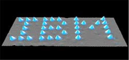
Using a Scanning Tunneling Microscope (STM), IBM researchers Donald Eigler and Erhard Schweizer were able to arrange individual Xe atoms on a surface.
Although the process was painstakingly slow, the remarkable image allowed researchers to place individual xenon atoms with nanoscale precision and to visualize the results.
This now famous image of the atomic world “hangs” in IBM’s STM Image Gallery, and demonstrates early attempts to create structures one atom at a time.
(Nature, 344, 524, 1990)
Carbon Nanotubes
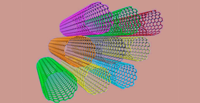
In 1991, Sumio Iijima at NEC in Japan discovered a new form of carbon called nanotubes, which consisted of several tubes nested inside each other.
Two years later, Iijima, Donald Bethune at IBM in the US, and others observed single-walled nanotubes just 1-2 nanometers in diameter. Nanotubes behave like metals or semiconductors but can conduct electricity better than copper, transmit heat better than diamond, and are among the strongest materials known.
Nanotubes could play a pivotal role in the practical applications of nanotechnology if their remarkable electrical and mechanical properties can be exploited.
(S Iijima, Nature, 354, 56, 1991)
1996: Using DNA & Gold Colloids to Assemble Inorganic Materials
Since Faraday’s discovery of the unique electronic and optical properties of gold colloids in 1857, researchers have sought to harness these capabilities.
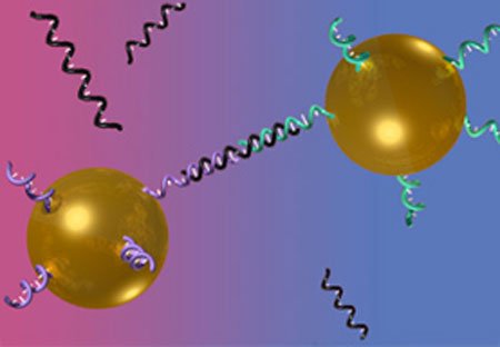
In 1996, Northwestern University researchers Chad Mirkin and Robert Letsinger discovered a way to do this. They attached strands of synthetic DNA onto gold nanoparticles. Since complementary strands of DNA can recognize and bind to each other, the DNA served as a blueprint, a construction worker, and a sorter to create new inorganic materials.
By manipulating the DNA, they were able to make materials with the same unusual properties as the nanoscale building blocks that they are made from. This advance generated an explosion of interest in making designer bio-inorganic architectures at the nanoscale.
(Nature, 382, 607-609, 1996)
1999: Development of Dip-Pen Nanolithography
A pivotal development in the constellation of nanotechnology tools was Dip-Pen Nanolithography (DPN).
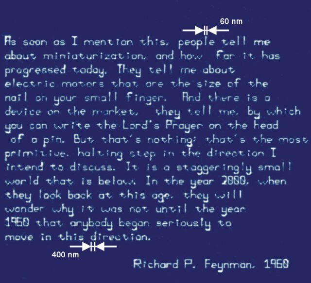
Invented by Chad Mirkin at Northwestern University, the concept is based upon a classic quill pen – a 4,000-year-old technology. Using an atomic microscope tip, DPN allows researchers to precisely lay down or “write” chemicals, metals, biological macromolecules, and other molecular “inks” with nanometer dimensions and precision on a surface.
DPN has progressed to include 1,000,000 tip serial and parallel processing – opening the door to credible nano-manufacturing techniques for smaller, lighter weight, faster, and more reliably produced electronic circuits and devices, high-density storage materials, and biological and chemical sensors.
(Science, 283, 661, 1999)
2000: Feedback-Controlled Lithography (FCL)
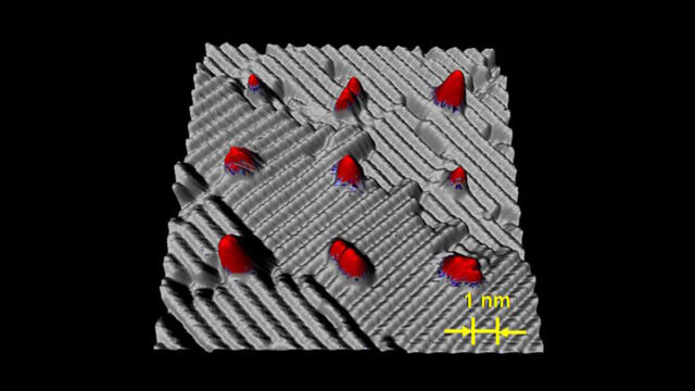
Feedback-controlled lithography (FCL) is a technique that allows researchers to use the Scanning Tunneling Miscroscope (STM) to precisely and selectively build structures at the nanoscale.
Developed by Mark Hersam (Northwestern University) and Joseph Lyding (University of Illinois at Urbana-Champaign), FCL is conducted by first coating a silicon sample with hydrogen (otherwise known as hydrogen passivated silicon).
Using the STM, researchers can then image (or see) the surface of the silicon sample. When an electric voltage is applied to the STM tip from an outside source, the silicon-hydrogen bonds are broken. By controlling the position of the STM tip, hydrogen atoms are thus removed with atomic precision.
This technique allows fundamental studies of chemistry at the single molecule level and has opened the door for building prototype electronic devices and other structures at the nanoscale.
(Jour. Vac. Sci. Tech.A, 18, 1349, 2000)
Establishment of National Nanotech Initiative

Attempts to coordinate work on the nanoscale began in November 1996 when staff members from several federal agencies decided to meet regularly to discuss their plans and programs in nanoscale science and technology.
By 1998, this group (now called the Interagency Working Group on Nanotechnology or IWGN) was focused on defining the art of nanoscale science and technology and forecasting possible future developments.
In August 1999, IWGN completed its first draft of a plan for an initiative in nanoscale science and technology. The plan went through an approval process involving the President’s Council of Advisors on Science and Technology (PCAST) and the Office of Science and Technology Policy.
As a result of this work, the Clinton administration raised nanoscale science and technology to the level of a federal initiative by including major funding as part of its 2000 budget submission to Congress, and officially referred to it as the National Nanotechnology Initiative (NNI).
(AIP Bulleting of Science Policy News)