With the dawn of the 20th century came the development of several instruments and theories that are essential to nanoscience researchers today.
From electron microscopes to modern computers, the pace of discovery was incredible.
1908: Mie Theory
German physicist Gustav Mie played an important role in nanotechnology with his theory of light scattering by particles — but it would be several decades before we could take advantage of it.
His theory shows that light scatters from particles more efficiently at short wavelengths than at long wavelengths. For example, we see the sky as being blue because molecules in the air, which are extremely small particles, scatter light from the sun more efficiently for blue light than for yellow or red, as blue light has the shorter wavelength. When the sun sets, the sunlight travels through the atmosphere over a longer distance than when it’s overhead.
The most important scattering in this case arises from dust particles. These particles still scatter light more effectively for blue colors, so the light that is not scattered is a mixture of red and yellow. This produces the characteristic red color of the setting sun.
Mie Theory helped scientists to realize that the size of particles determines the colors that we see. Mie went on to develop a way to calculate the size of particles by determining the light scatter. For nanoparticles and larger particles, this theory requires a huge number of calculations, so it was rarely used until about 20 years ago when supercomputers became available. Now, Mie Theory (as well as others developed more recently) helps researchers predict and determine the size of nanoparticles.

1931: First Electron Microscope
Although light microscopes have been around since the Renaissance, they were unable to recognize objects that were smaller than the wavelength of visible light (0.4-0.7 micrometers) until the early 20th century.
To see particles smaller than this, scientists had to bypass light altogether and use a different sort of “illumination,” one with a shorter wavelength. In 1931, German scientists Max Knott and Ernst Ruska developed an entirely new type of microscope that would eventually reveal a new “small” world.
With the electron microscope, electrons are accelerated in a vacuum until their wavelength is extremely short, only one hundred-thousandth that of white light. Beams of these fast-moving electrons are focused at a sample. Some parts of the sample soak up the electrons, while other parts scatter them. An electron-sensitive photographic plate “records” this action and creates an image.
By 1933, the electron microscope was able to exceed the detail and clarity of the traditional light microscope. This was an important first step in the development of techniques and instrumentation that would eventually enable research at the nanoscale.
(Knoll, M. and Ruska, E.; Ann. Physik 12, 607-640 and 641-661, 1932, submitted 10 September 1931)

1947: The Transistor
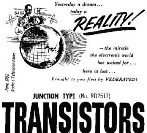
Until the mid-1940s, vacuum tubes were the state-of-the-art in electronics.
Capable of converting alternating current to direct current (AC to DC) and amplifying an electronic signal, vacuum tubes were used in everything from switching telephone calls to building the first high-speed computer, ENIAC.
But the limitations were clear. Vacuum tubes were bulky, and to make more powerful computers, more tubes were needed. (17,000 tubes were used in ENIAC!) Tubes were also fragile and overheated easily.
In 1945, Bell Labs established a research group to look into finding a solution. The group was led by William Shockley and included Walter Brattain and John Bardeen. After two years, Bardeen and Brattain created an amplifying circuit that seemed to work, using the element germanium. They called it the point-contact transistor.
The discovery did not gain attention until 1951, when Shockley improved upon the original idea with a junction transistor. The transistor was a solid (giving rise to the term “solid-state technology”), but had the electrical properties of a vacuum tube. Furthermore, it was inexpensive, sturdy, used little power, worked instantly, and, best of all, was tiny.
The three men shared the 1956 Nobel Prize in physics for “their researches on semiconductors and their discovery of the transistor effect.”
The invention of the transistor and the integrated circuit marked the beginning of microelectronics, a field that relies on tools for miniaturization. The semiconductor industry is one of the largest technology drivers in the field of nanotechnology. Researchers today are looking to enable the creation of chips holding billions or even trillions of nanoscale transistors.
(US Patent 2,569,347, Sept. 25, 1951, applied for June 26, 1948).
1950: Tunneling Phenomenon
In 1958, Leo Esaki, a Japanese physicist working at Sony Corporation, discovered that electrons could sometimes “tunnel” through a potential barrier formed at the junctions of certain semiconductors even though classical theory predicted that this was not possible.
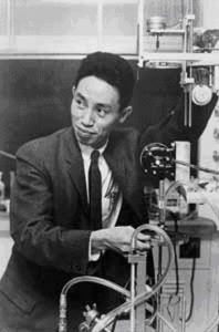
What Dr. Esaki observed was an example of how materials at the nanoscale are controlled by different laws of behavior, i.e. they are controlled by quantum mechanics as opposed to classical physics.
The discovery lead to the creation of the tunneling diode (sometimes called the Esaki diode), an important component of solid-state physics, and the first time that tunneling (an important nano-electronics phenomenon) was used in a real device.
Dr. Esaki was awarded the 1973 Nobel Prize in physics for this discovery along with physicists Ivar Giaver of Norway and Brian D. Josephson of Great Britain.
(L. Esaki, Phys. Rev., 109, 603, 1958)
1951: Erwin Mueller’s Field-Ion Electron Microscope
The development of nanotechnology was, and is, dependent upon advances in scientific instrumentation.
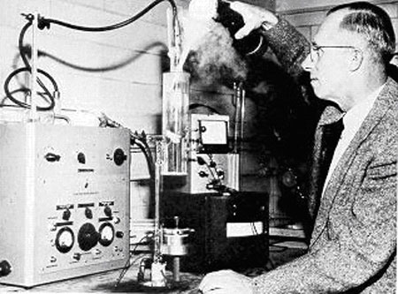
Erwin Mueller, a professor at Penn State University’s department of physics, made an important contribution when he invented the field-ion electron microscope in 1951. For the first time in history, individual atoms and their arrangement on a surface could be seen.
For this accomplishment, Professor Mueller is known as the first person to “see” atoms. The device was a landmark advance in scientific instrumentation that allowed a magnification of more than 2 million times.
Born in Berlin in 1911, Erwin was the only child of a family of modest means. His father was a construction worker who specialized in plastering ceilings in houses. He obtained his doctorate in engineering from the Technische Hochschule Berlin-Charlottenburg in 1936. Erwin was recruited by Penn State. He and his family moved there in 1952 and he became a US citizen in 1962. His achievements were recognized by numerous awards, including election to the prestigious National Academy of Sciences.
(Mueller, E.W., Zeitschrift fuer Physik, 131, 136, 1951).
1953: Discovery of DNA
One of the landmark achievements in the 20th century was the discovery of DNA. By the 1950s, scientists already knew that DNA – deoxyribonucliec acid – carried genetic information, but they didn’t know what it looked like or how it worked.
In 1953, Dr. James Watson and Professor Francis Crick published an article in Nature describing the double helix structure of DNA. They showed that when cells divide, the two strands that make up the DNA helix separate and a new “other half” is built on each strand, a copy of the one before. This means that DNA can reproduce itself without changing its structure, except for occasional errors or “mutations.”
James Watson, Francis Crick, Maurice Wilkins, and Rosalind Franklin all played critical roles in this discovery of the DNA structure.
In 1962, Wilkins shared the Nobel Prize with Watson and Crick. Tragically, Rosalind Franklin had died a few years earlier at the age of 37, and since Nobel Prizes are not awarded posthumously, she was not included in the honor.
Decades later, DNA’s ability to self-assemble into tiny structures would inspire researchers to use the same principles to develop nanoscale structures with specific dimensions and chemical properties.

1959: Feynman Points the Way Forward
Richard P. Feynman is often credited with predicting the possibilities and potentials of nano-sized materials.
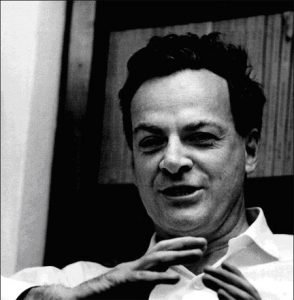
Feynman gave a talk on Dec. 29, 1959 entitled, “There’s Plenty of Room at the Bottom.” In his speech, he stated:
“What I want to talk about is the problem of manipulating and controlling things on a small scale. As soon as I mention this, people tell me about miniaturization, and how far it has progressed today. They tell me about electric motors that are the size of the nail on your small finger. And there is a device on the market, they tell me, by which you can write the Lord’s Prayer on the head of a pin.
“But that’s nothing; that’s the most primitive, halting step in the direction I intend to discuss. It is a staggeringly small world that is below. In the year 2000, when they look back at this age, they will wonder why it was not until the year 1960 that anybody began to seriously move in this direction.”
Feynman would go on to win the Nobel Prize in physics.
(Feynman, R.P. American Physical Society Meeting, Pasadena, CA, Dec. 29, 1959)
1960: Ferrofluids
In the 1960s, NASA researchers were trying to find ways to control liquids in space.
They discovered that nano-sized magnetic particles of iron that were given a chemical coating, or surfactant, that prevented them from clumping together could be dispersed in oil or water. They could then control the location of the fluid (called a ferrofluid) with a magnet.
On Earth, ferrofluids are used inside loudspeakers, where they help keep the inner parts cool. They are also used on computer hard drives and in semiconductor manufacturing, as seals to keep out the dust and other contaminants.
Nanotechnologists want to harness ferrofluids for other important uses such as developing tiny sensors, or inside the body as biomedical devices to deliver drugs, absorb toxins, or treat hypothermia. It is even possible that ferrofluids could be used to help clean up hazardous waste spills.

1960: Zeolite Catalysts
A zeolite is an inorganic porous material which works as a kind of molecular sieve – allowing some molecules to pass through while excluding or breaking down others. Zeolites can be natural or synthetic, and new zeolites are still being discovered and invented.
In 1960, Charles Plank and Edward Rosinski developed a process to use zeolites to speed up chemical reactions. Plank and Rosinski’s process focused on using zeolites to break down petroleum into gasoline more quickly and efficiently.
Researchers are currently working to design zeolite catalysts at the nanoscale. By adjusting the size of the zeolite pores on the nanoscale, they can control the size and shape of molecules that can enter.
In the case of gasoline production, this technique could mean that we would get more and cleaner gasoline from every barrel of oil. It is hoped that nanotechnology will help reduce the cost and pollution associated with producing gasoline and other petroleum products.
(US Patent #3,140,249)

1965: Moore’s Law
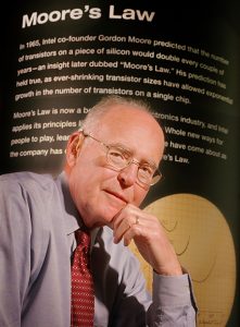 Writing for Electronics magazine in 1965, Gordon E. Moore, the founder of Intel Corporation, noted that the number of transistors per integrated circuit had doubled every two years.
Moore predicted that this trend would continue for another ten years, and his prediction was quickly dubbed “Moore’s Law” by the press.
Moore’s prediction turned out to be prophetic. In fact, the complexity of a chip continued to double yearly, long after 1975. The rate of doubling has only recently slowed to about every 18 months.
Many researchers believe that devices which use electronic nanotechnology and molecular electronics will keep Moore’s Law accurate into the future.
(Electronics Magazine, 38, 114-117, 1965)
1970: Sir John Pople’s Software
Mathematics is a foundation for science; it provides mathematical descriptions of complex real-world phenomena, or “models.”
Modeling develops hand-in-hand with the science it describes. Developing new mathematical formulas is an essential part of science, and as science becomes more complicated, new, faster formulas are needed.
Although computers had become dramatically more powerful by 1970, new software had to be developed in order for that power to be useful. Up until this time, it was very difficult to solve the complex mathematical equations needed to determine the properties of molecules.
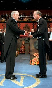
In 1970, John Pople and his research group developed Gaussian, a software program that would perform these calculations. This pioneer in the use of computers to predict the behavior of atoms and molecules also developed many of the algorithms that made computer-based modeling at the nanoscale possible.
For his work, Dr. Pople, a Northwestern University Board of Trustees professor and British citizen, shared the 1998 Nobel Prize for chemistry and was knighted by Queen Elizabeth in 2003.
(Quantum Chemistry Program Exchange, Program No. 237, 1970)